Welcome to Wuhan Yoha Solar Technology Co., Ltd!
common problem
Site Map
Language:
 Chinese
 English
Welcome to Wuhan Yoha Solar Technology Co., Ltd!
common problem
Site Map
Language:
Chinese
English
| Brand: | YOHA Solar |
| Model: | YHZD-ELIV |
| Unit: | unit |
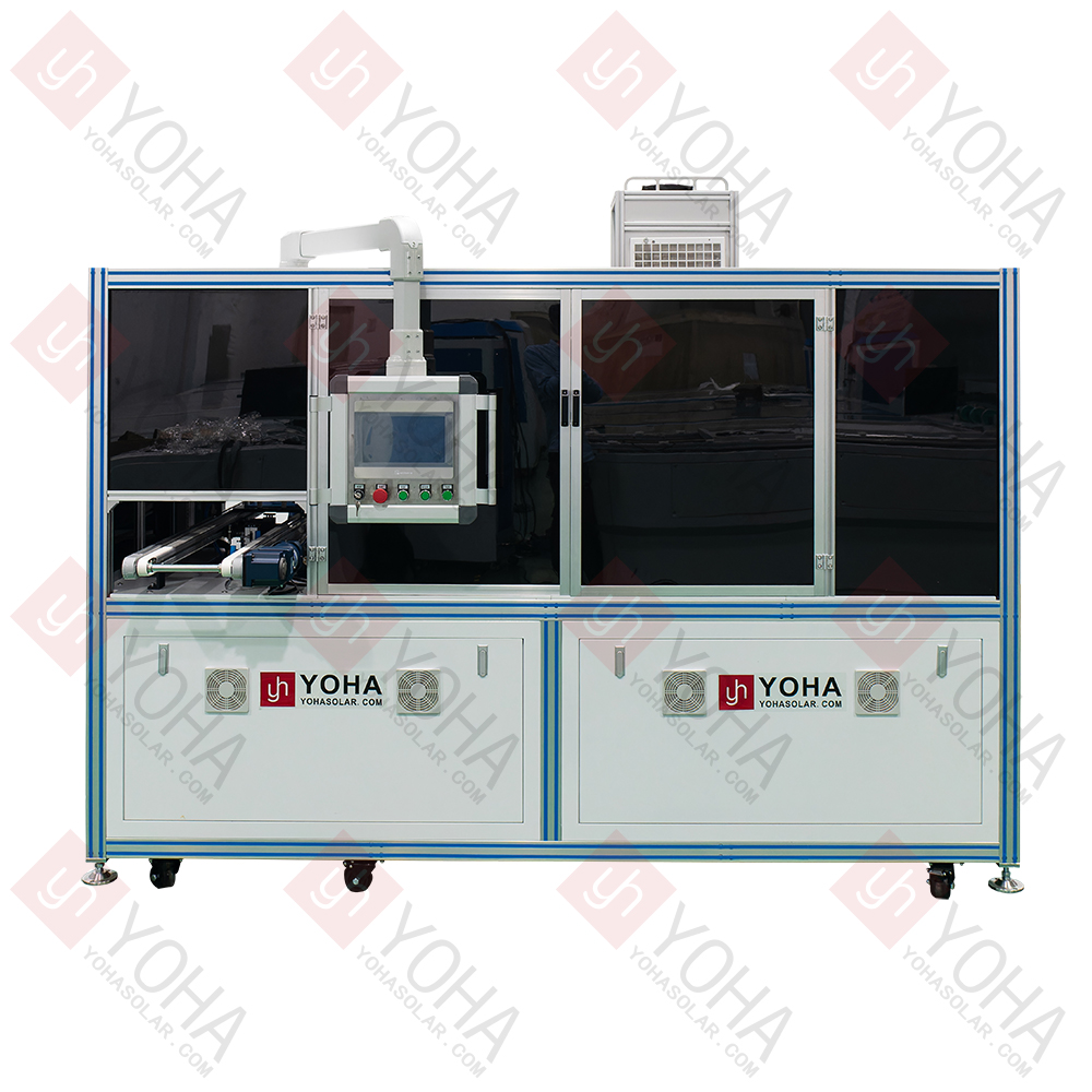
The Automatic Solar Wafer EL+IV Integrated Tester is a highly integrated, advanced inspection equipment specifically designed for the photovoltaic industry. It efficiently and precisely performs online quality inspection and performance evaluation of solar wafers. Innovatively combining EL (Electroluminescence) defect detection and IV (Current-Voltage characteristic) performance testing functions into a single automated platform, it utilizes robotic arms or conveyor belts for automatic loading/unloading. The wafers are sequentially guided through the EL imaging system in a darkroom environment and the IV testing station. This process simultaneously captures internal defect images (such as micro-cracks, broken fingers, and fragments) and key electrical performance parameters (efficiency, open-circuit voltage, short-circuit current, fill factor, etc.). This equipment significantly enhances inspection efficiency and consistency, serving as a core tool for quality control, process optimization, and binning/sorting during wafer production, ensuring products meet high standards.
1. Dual-Function Integration: EL detects defects (micro-cracks, sintering issues), IV measures performance (efficiency, power).
2. Full Automation: Automatic loading/unloading, positioning, testing; seamless integration with production lines.
3. High Efficiency & Precision: High-speed testing (typically up to thousands of wafers/hour), high-resolution EL imaging.
4. Intelligent Analysis: Software automatically identifies defects, performs binning, and generates reports.
5. Process Closed Loop: Real-time data feedback guides production adjustments, improving yield.
| Item | Specification |
|---|---|
| Model | YHZD-ELIV |
| Wafer Specification | Compatible with Mono-crystalline, Multi-crystalline, PERC, HJT, TOPCon, etc. |
| Camera Resolution | 5 Megapixels |
| Camera Type | Custom High-Definition Industrial Camera |
| Testing Orientation | Vertically Downward |
| Light Source | Complies with IEC 60904-9:2020 Standard |
| Irradiance Instability | ≤2% |
| Irradiance Non-Uniformity | ≤2% |
| Single Flash Pulse Duration | 10ms |
| Throughput | 2000~5000 Wafers/Hour |
| Breakage Rate | ≤0.05% (Grade A Wafers) |
| Sensitivity | Capable of detecting cracks narrower than 0.03mm |
| Loading Method | Automatic Loading/Unloading |
| Effective Testing Area | 230*230mm |
| Binning Cassettes | 8 Binning Cassettes (Optional) |
| Function Expansion | Can be equipped with AOI/PL inspection functions |
Temperature & Humidity: Maintain constant temperature (recommended 23±2℃) and humidity (40%~60% RH) to avoid temperature drift affecting IV test accuracy.
Cleanliness: Dust-proof and anti-static. Dust can cause poor probe contact or EL imaging misjudgment.
Darkroom Requirement: Complete darkness is required during EL testing (ambient light < 5 lux) to avoid light source interference with imaging.
Daily Calibration: Calibrate IV test using standard wafers (open-circuit voltage, short-circuit current) before use, ensuring data traceability to national standards.
Probe Maintenance: Regularly clean probe surface oxidation layer. Check for uniform pressure (typically 0.1~0.3N required) to prevent wafer scratching or poor contact.
Lens Maintenance: Clean EL camera lens weekly with lint-free cloth to avoid stains blocking defect recognition.
Wafer Placement: Ensure wafers are flat without warping. Robotic arm suction cup air pressure must be adapted to wafer thickness (low pressure for thin wafers to prevent breakage).
Test Parameter Matching: IV test current range and scan speed must match wafer type (e.g., HJT requires low current range, TOPCon requires fast scan speed).
Avoid Over-Testing: EL test duration should not be too long (typically < 3 seconds) to prevent wafer overheating or luminescence decay.
Electrical Safety: IV testing involves high-voltage modules (up to 30V). Grounding must be reliable. Wear insulated gloves during operation.
Mechanical Protection: Do not extend limbs into conveyor belt/robotic arm areas during operation. Emergency stop button must remain accessible.
Laser Safety: Do not look directly into positioning lasers (Class 2 or below) to avoid retinal damage.
Data Backup: Back up original EL images and IV curves daily to prevent data loss.
Software Updates: Regularly upgrade defect recognition algorithm libraries (e.g., adding new models for broken fingers, PID) to improve detection rate.
Access Control: Parameter modification permissions restricted to engineers only to avoid operational errors causing batch data anomalies.
TOP
18086473422
MESSAGE